ECE 385 - Digital Systems Laboratory
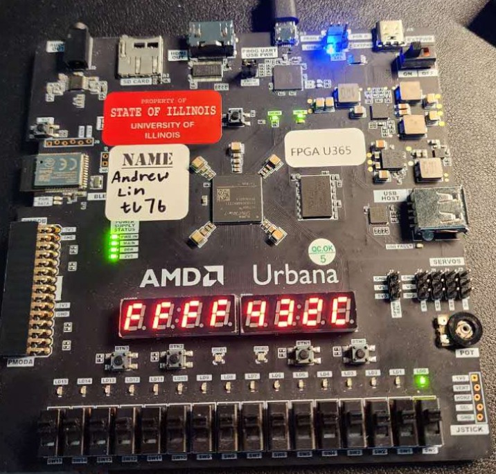
FPGA-based hardware design and computer architecture.
Course Labs
MicroBlaze SoC & Ball Game
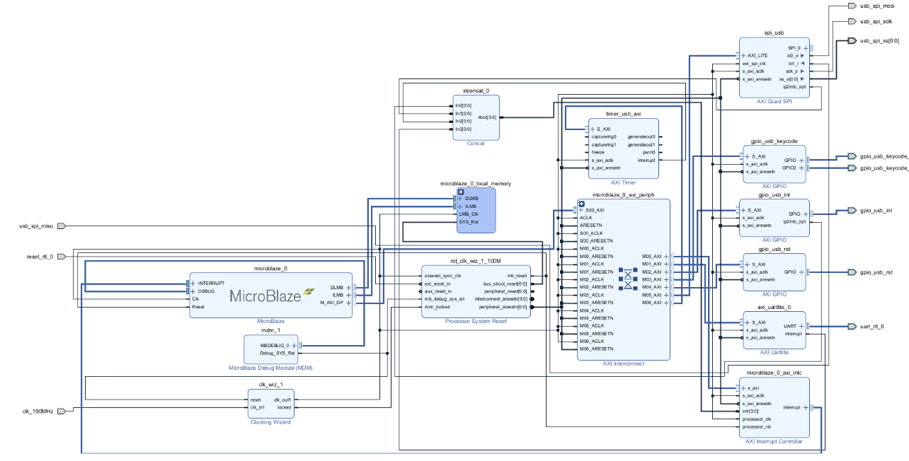
◦ Setup: MicroBlaze softcore processor with pre-made AXI IP blocks, programmed in C.
◦ I/O: USB hosting via SPI + MAX3421E, UART terminal, GPIO memory-mapped I/O, and VGA-to-HDMI output driving a keyboard-controlled ball game.
◦ HDMI Display: AXI-based HDMI interface IP with built-in VRAM — control registers stored on registers for the first version, then moved to BRAM.
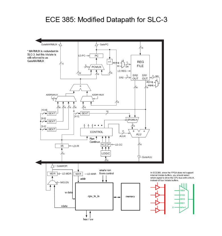
SLC-3 Processor
◦ Design: Simplified LC-3 ISA (ADD, AND, NOT, load, store) with eight registers, memory-mapped switches/hex display at xFFFF, and 3-cycle memory timing.
Arithmetic Building Blocks
◦ Units: Full, look-ahead, and select adders plus a hardware multiplier on FPGA.